Successful engineering of a thin film structure through semi-modern manufacturing techniques was first reported as early as the 1800s. Oil-sealed vacuum pumps were used to sputter a component substrate with nebulized sample material, forming an extremely functional coating in a thin film. This form of physical vapor deposition (PVD) was one of the earliest and most important precursors to modern vacuum deposition techniques for nanofabrication and nanoscale surface engineering.
Brief History of Thin Film Engineering
Perhaps more important than this thin film sputtering technique was the rudimentary vacuum technology provided by the oil-sealed pump itself. Edison used this type of tool in 1887 to evacuate the first carbon-filament incandescent lamps and reduce the oxygen content within a bulb so that a filament could reach white-hot temperatures without catching fire.
The problem with early PVD processes was the inability to achieve true vacuum conditions prior to deposition. Ensuring that a substrate is uniformly coated by a thermal vaporization source without contamination requires the processing chamber to be free from residual gas molecules. Sputtered material travels along a line-of-sight trajectory which can be interrupted by collisions with unwanted gaseous molecules in the deposition chamber. This complicated early PVD processes, and thus vacuum deposition of thin film structures was not considered commonplace until the early 20th Century.
Modern Thin Film Engineering
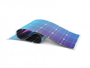
PVD thin film engineering is now broadly used for nano-engineering of microelectronics, organic photovoltaic cells, precision optical equipment, functional textiles, innovative display technologies, and much more. This has been enabled by the widespread utilization of additional deposition techniques that operate on bottom-up or top-down synthesis methods.
Bottom-up synthesis of thin film structures involves the subsequent deposition of atoms to lithographically build a thin film on the substrate. Top-down synthesis, by contrast, refers to a process where thin films are cut out of a substrate using a technology such as ion beam etching (IBE). PVD is a typical bottom-up form of thin film engineering, while IBE operates by sputtering a substrate with an ion beam to dislodge the atoms of a substrate around a pattern dictated by a developed photoresist.
Thin films are now ubiquitous in modern life, but process control is still complicated by the same problems that troubled early adopters of the technology. Enhancing thin film manufacturing processes with spectrometry capabilities enables manufacturers to guarantee that any special parameters are met with outstanding batch-to-batch reproducibility. This may require residual gas analyzers (RGAs) to characterize optimal vacuum conditions in the processing environment and provide insight into the partial pressures of residuals such as gaseous hydrocarbons and volatile organic compounds (VOCs).
The HPR-30 Series from Hiden Analytical is a vacuum process analyzer for gas and vapor sampling systems. It has been engineered for maximum response sensitivity and speed for in-situ monitoring of residuals in numerous thin film engineering techniques.
Post processing with secondary ion mass spectrometry (SIMS) can also provide valuable insight into the quality of thin film structures on the angstrom scale. This technology sputters the uppermost surface material of engineered coatings and analyzes the ejected secondary ions to determine elemental composition with nanometer depth resolution. Hiden Analytical provides both static and dynamic SIMS capabilities for accurate chemical imaging of thin film surfaces at thicknesses exceeding 30 microns, and as small as a single monolayer.
Hiden Analytical and Nanofabrication
Hiden Analytical is a leading supplier of quadrupole mass spectrometers for academic and industrial applications. We have developed an extensive range of research tools for process optimization, quality control, and research into the fabrication of functional thin film structures.
If you would like more information about our expertise in thin film please do not hesitate to contact us.